Lab 2 Writeup
Lab 2: Multiplexed 7-Segment Display
Hours Spent: 13.5, Mapped with Toggl Track
Introduction
In this lab, a design was developed to display the output of two 4-pin DIP Switches on a dual seven segmenet LED matrix, such that each four-pin switch was mapped to one display. The sum of these two values was then displayed on a set of five LEDs. The dual seven segment display is lit up using the same function as in Lab 1. Resultantly, it was necessary to multiplex the dual segment such that only one common anode was powered at a time. In addition, due to the current draw required on the display, the +3.3V regulator on the E155 Board was used to power the seven segment display (with the assumption that a computer would be able to supply the required amount of current). In addition, to prevent the current from flowing directly through the FPGA, the common anode was turned on and off using a PNP transistor setup. The LED display needed to be breadboarded, as well, because there are only a total of 4 FPGA-controllable LEDs onboard the development board. A 10-LED display was used to show the sum of each of the bits for this program.
Design: Modules and Testbenches
Modules
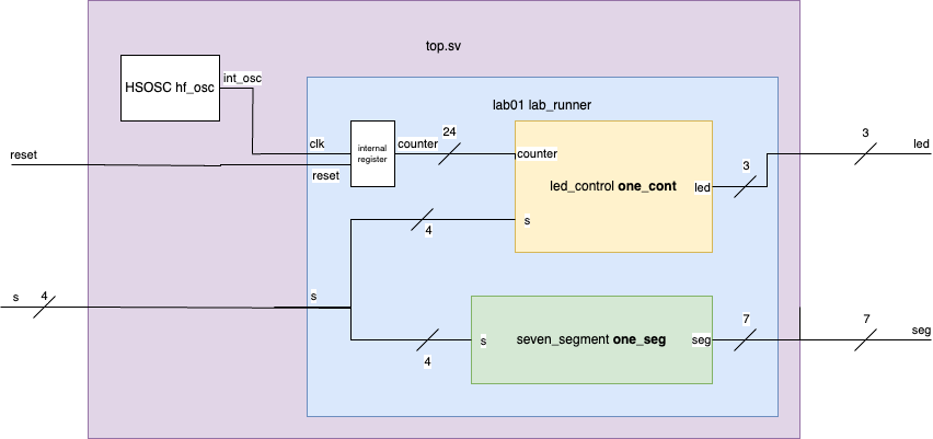
From the top layer down, it was understood that there would be the blocks displayed in the diagram depicted below.
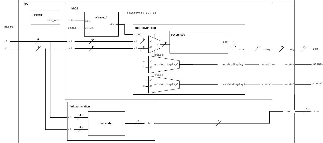
When encoded, the lab resultantly consisted of the above modules. They are explained in the table (Table 1) below.
| Module Name | Module Function |
|---|---|
top.sv |
Puts together lab2. Generates a clock that will run the program, and outputs variables to the necessary pins. |
lab02.sv |
Runs an always_ff block to determine the current state and the next state of the system. Runs combinational logic blocks of dual_seven_segment and led_summation for required seven segment and led logic |
dual_seven_seg.sv |
Calls on the seven segment block from Lab 1. According to the clock’s counter, half the time will return seven segment for one switch, and half the time will return the seven seg output for the other |
seven_segment.sv |
Uses combinational logic to determine which seven segment cathodes to turn on, and which to turn off. |
led_summation.sv |
Adds together the collected 4-bits of the two switches and returns their binary equivalent as a 5-bit array |
Some important notes about this layout is that the clock is used to determine a state, S0 or S1, which will determine which display is turned on at any given time. In state S0, the system would rely on one switch (s1); in this case, seven_segment would be called on for that switch only. The system would then turn a corresponding anode on and off using the PNP resister; in this case, since its a PNP resistor, it needed to be turn “off” to turn the system on. In state S1, the output of seven_segment instead relies on the output of switch s2, and will return the opposite output for the anode display. The logic for this can be found in Table 2, the following can be said for each of the states.
| state | Switch Used for Seven Segment Logic | Anode 1 | Anode 2 |
|---|---|---|---|
| S0 | s1 | 0 (i.e. Display 1 is on) | 1 (Display 2 is off) |
| S1 | s2 | 1 | 0 |
| X | an error has occured, s = 0 | 1 | 1 |
Once these modules were all written, they were compiled, checked for errors, and finally put into Questa for testing.
Testing
Two test benches were written for this lab. The first one checks to make sure that lab02.sv as a whole can run, and correctly lights up the LEDs as seen fit. Because direct control of the counter can’t be gotten when calling on this upper-level module, the testbench instead only checked that at least one of the outputs of the potential seven segment outputs was correct. The second was used to determine that the proper segment was lit up when the correct switch/state was entered into the dual_seven_seg module. In the case of both, a testvector file was composed and assembled using Python to make sure that all possible options were checked for and confirmed. This Python program can be found in Github, at this_file.py
Testbench lab02_tb
In order to make sure that all cases were covered, the test vectors were created by running a for-loop to generate a series of switches; each of these switch combinations was used to generate a potential segment output, and finally a summation-vector was made that could be called on to correctly add the sum of both segments to the end. The python file then printed a series of strings of the form
switch1_switch2_segment1_segment2_summed led values
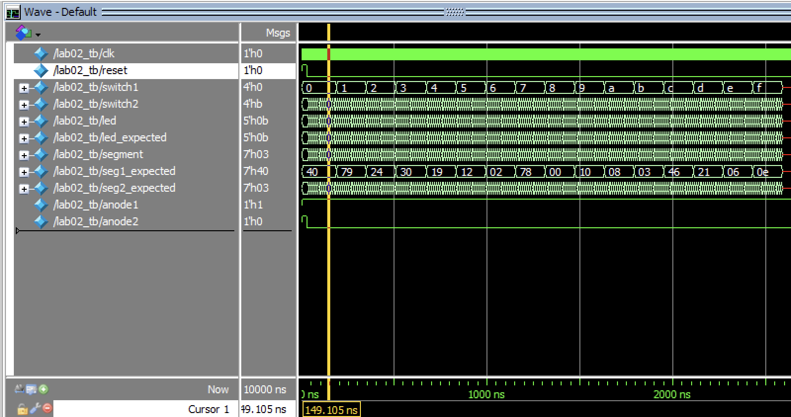
By running two for loops to cycle through all potential switch values, it can be confirmed that all potential values within the system have been reached. Within the test bench itself, the system uses an or expression to confirm that at least one of the segment outputs is equal to the segment output of the system. It also confirms that the led_summation is working as anticipated.
Using this testbench, confirmation of the functionality of the whole of lab02 was completed, as all tests could be run without failure (Figure 2)
Testbench dual_seven_seg_tb
In order to make sure that all cases were covered, the test vectors for this testbench were created by running a for-loop to generate a series of switches, similar to lab02 testbench. However, these nested for-loops were nested in one final for-loop, which acertained which state the system was in; each of these switch combinations was used to generate a potential segment output, and finally a summation-vector was made that could be called on to correctly add the sum of both segments to the end. The python file then printed a series of strings of the form
switch1_switch2_state_segment_anode1_anode2
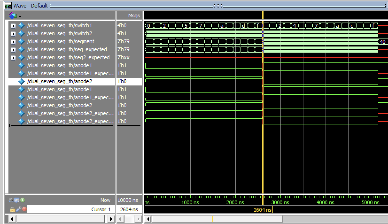
By running two for loops to cycle through all potential switch values, it can be confirmed that all potential values within the system have been reached. Within the test bench itself, the system uses an or expression to confirm that at least one of the segment outputs is equal to the segment output of the system. It also confirms that the led_summation is working as anticipated.
Using this testbench, confirmation of the functionality of the whole of lab02 was completed, as all tests could be run without failure (Figure 3)
With this confirmation that the logic of the modules were working, it was possible to then move on to physical implementation of the program on the actual FPGA and hardware.
Design: Seven Segment Display
The design was developed based on work from Lab 1. The same seven segmenet module was used within a double multiplexer, which used the clock to switch back and forth between powering the two common anodes of the dual display. Using multiplexing, the two values were displayed.
Because the final system was multiplexing between two segments, this means that the common anode of a given seven-segment LED must be able to be turned OFF. In the original design for the seven-segment display, the common anode had been plugged in directly to the +3.3V of the development board, and in this way circumvented being powered by the FPGA board (which can not supply more than 0.8 mA at a given time). Attempting to power the seven-segment display directly won’t work (as will be explained in Section 1.3.1) unless you want to short your board. Resultantly, two PNP 2N3906 transistors were used, wherein the FPGA was used only to turn the transistor on and off, allowing the +3.3V coming from the Development board to flow within the circuit (once again, circumventing using the FPGA as a current supply directly).
Calculations: PNP Transistor Circuit
Beforehand, to ensure proper requisites were met for powering the seven segment display that everything was properly set up for the PNP transistor and the resistors in the circuit, some simple mathematial calculations were performed to ensure proper voltage and current was kept throughout the circuit.
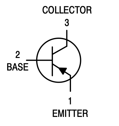
The transistors we were using were 2N3906 PNP transistors. PNP transistors have three terminals; the base, which controls if the PNP is on or off, the emitter, where electrons come from, and the collector, where the electrons go (Figure 4). For PNP transistors to work, there must be enough of a voltage gap between the base voltage and the emitter voltage that current can flow from one too the other; when this happens, current can also flow from the emitter to the collector, with the assumption that the voltages being used do not break or short out the transistor itself.
To determine these limitations, it was necessary to know three things: the voltage drop across the collector to the emitter (V_CE), the voltage drop across the base to the emitter (V_BE), and finally the maximum current draw that would flow from the collector to the emitter (I_CE).
According to the PNP’s datasheet, on average the V_CE drop is 3.3 V. The value of V_BE is, as with most transistors, assumed to be about 0.7 V. To start out with, the primary goal of this circuit should be to power the FPGA board without shorting it by sending too much current through it via the emitter to base connection on the board. Resultantly, a resistor should be placed between the FPGA’s output GPIO pin and the base of the transistor such that the current is less than the maximum possible current that can be sent into the board. This can be configured according to the datatable for the GPIO pins (Figure 5), where it can be seen that the maximum current that should be sent into or out of the FPGA board is 0.8 mA. The maximum current we will be sending into our board is based on the resistor values that we install for the diodes with the dual segment display. With the assumption that we use the same 220 Ohm resistors we were originally using, the current draw through each of these resistors will be slightly reduced from what was considered in Lab 1.

First and foremost, I intend to power the LED’s using 3.3V, but these volts will first travel across the transistor, which is dependent on the current I_C traveling through the circuit. Assuming that this is relatively negligable (see Figure 15 on the PNP Datasheet, to observe that most of the Voltage removed for current lying under 60 mA is close to 0.1 V), and knowing that per diode line there will be an anticipated voltage drop of 2.1 V, that means that any one resistor will need to remove 3.3 - 2.1 Volts, or 1.2 V, from the circuit. When traveling across a 220 Ohm resistor, this will result in a current of roughly 5.45 mA. Assuming that we’ll be powering seven segments at any one time (the maximum amount possible), this means that the total current draw that can be expected is 38.18 mA. We can then compute the necessary amount of current, I_B, that will need to travel through the base in order to turn this circuit on. Using the gain terms found in the datasheet (Figure 6), it can be seen that for a given current I_C = 40 mA, the gain will be roughly 50 around room temperature.
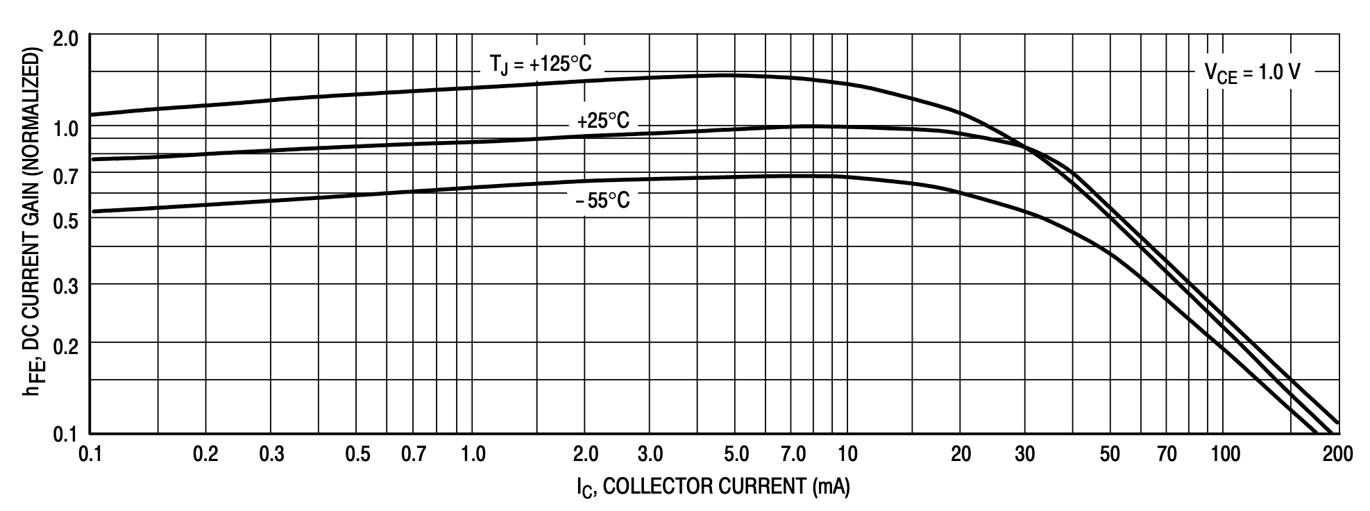
This means that the corresponding current I_B for the circuit is 38.18 mA/50 = 0.69 mA. In the case of I_B, there is only one resistor between it and the +3.3V power supply; in addition, the transistor will remove V_BE from the circuit, which means that the resistence of this component must be roughly (3.3V - 0.7V)/(0.69 mA), or 3.745 kOhms. In my final circuit design, I used a 3.3 kOhm resistor as it was the closest one I could find in lab, meaning that the final current draw was likely 0.07 mA, which still falls far under the maximum current that the FPGA board can use.
Table 3 below shows all the calculated voltages, currents, and resistances used for this circuit.
| Component/Measurement | Calculated Value |
|---|---|
| V_CE (voltage from Emitter to Collector) | 3.3 V |
| V_BE (voltage drop from Base to Emitter) | 0.7 V |
| I_C (anticipated current drawn from the emitter to the collector) | 38.18 mA |
| h_FE (DC gain relative to current I_C) | 55 |
| I_B (current necessary to turn on the PNP transistor) | 0.69 mA |
| R_transistor (current-limiting resistor between the FPGA and the emitter) | 3.745 kOhms |
Hardware Setup of Seven Segment Display
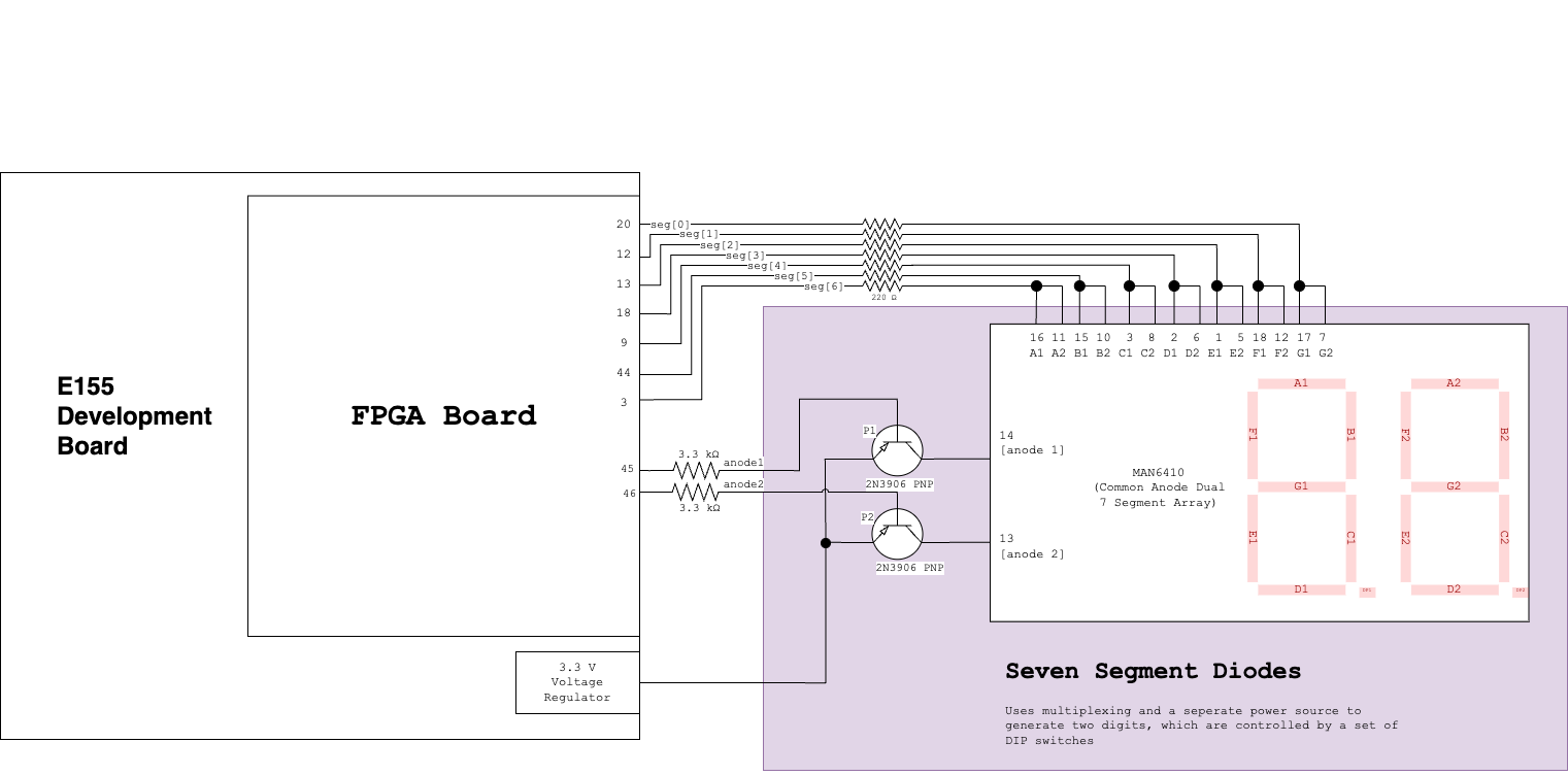
Similar to the previous Lab, in this lab each individual seven segment display was connected to a common anode (in this case, the output emitter of a PNP transistor). Each of the cathodes was attached via a resistor to the FPGA output pins onboard the E155 Breadboard Adapter. In similar fashion to what was described in Lab 1, setting the board up such that each cathode has a resistor allows for each of the diodes to be equally bright, as they all start at the same voltage drop and resultantly will draw the same current if powered (current being directly correlated with their lumosity).
The pin numbers, besides pin D, were kept the same as Lab 1 (it was later realized that the print of Pin 18 looks extremely similar to Pin 10, and that was why the system wasn’t working when Pin 10 was being powered; the system now works where Pin D is assigned to Pin 18). There are only three fundamental differences: two common anodes, two sets of A-G pins, and the presence of transistors within the circuit.
Common Anodes
The dual display had two common anodes, which were how control over multiplexing was done. At any one time, there were two “states” assumed to exist within the system; in one state, the display on the right was turned on (S0), and in the other, the display on the left (S1)
Two Sets of Pins
Since only a single module calculating the seven-segmenet display could be used at any one time, the corresponding pins of each cathode were connected to each other (i.e. A1 was connected to A2, B1 to B2, etc.). This meant that if both the common anodes had been lit up at the same time, both displays would show the same value, rather than only one lighting up.
Transistors
The common anodes were controlled via the PNP transistors. In doing so, it was possible to only light up one display at a time, while only performing one calculation of the seven segment display.
The final schematic of this system can be seen in Figure 7
Design: DIP Switch Pins
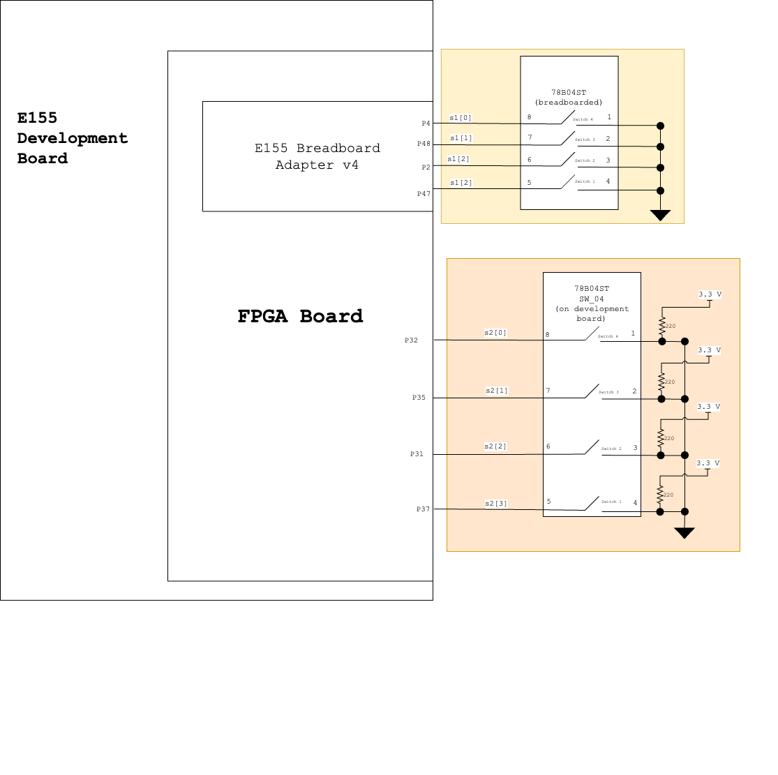
There are two DIP switches used in this lab, one that is breadboarded and controls the output of the rightmost display, and one that is soldered onto the E155 board and is used the left-most display. The same logic as the previous labs applies to both DIP switches, where the rightmost pin is used as the lowest-order bit. The on-board DIP switches did not require any additional resistrs, as there is an integrated pull-up resistor as detailed on the “E155 FA Development Board Datasheet”. However, the readboarded switches did not have these pull-up resistors already; after reviewing the 78B04ST DIP switch datasheet, it was found that the switches work at 3.3V, so no voltage adjustment was necessary. However, four additional 220 Ohm resistors were added to the switch board between the switch and ground to create a pull-up resistor, and then four FPGA GPIO pins were connected into the anodes of each DIP switch. The final connections for these connections, as well as the variables to which they were assigned can be found in Figure 8
Design: LED Counter
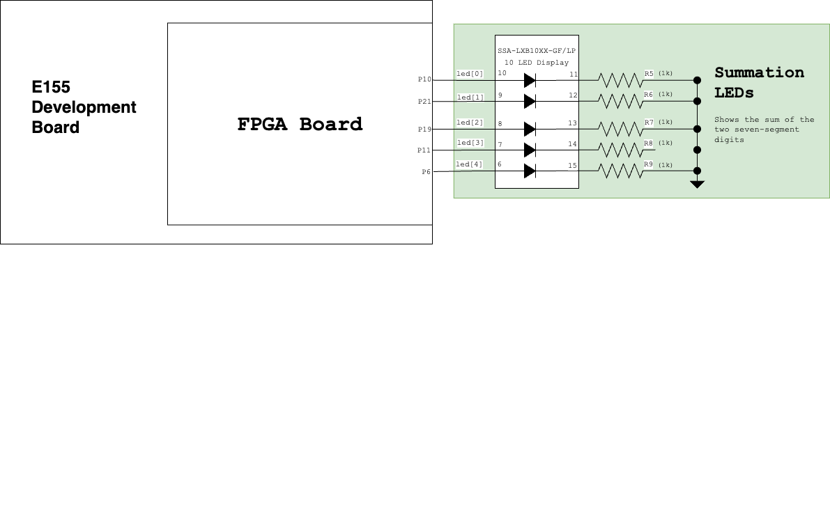
The final necessity for this lab is a set of five LEDs to display the binary summation of the two switches. For this project, a SSA-LXB10TW-GF-LP was used. Since the LED’s require a 2.1 voltage drop across them, very similar to the LEDs inside the seven segment array, 220 Ohm resistors were used for each LED while they drained to ground. This resulted in the corresponding schematic (Figure 9). Only 5 of the 10 LED-Diode Display were used.
Design: Overall
The final circuit is mainly controlled by the FPGA, except for the 3.3V that supplies the current for the seven segment voltage. The final circuit can be seen in Figure 10.
Results and Discussion
As shown in the two test bench simulations above, the program is able to receive the desired outputs. When observed in the lab, with hardware, the correct behavior can be similarly observed.
If future development desired, additional phases or multiplexed digits could be added quite easily, especially if scaled by 2, as the multiplexing is controlled by each digit of counter; hypothetically, if an additional two numbers needed to be added, two more switches could be set up on the breadboard in similar fashion, the counter could be assigned based on the state of two bits within counter (for a total of four states, rather than two), and the multiplexing would occur via four PNP transistors that move to four common anodes. Scaling is extremely possible with this design.
Conclusion
In conclusion, all of the program works properly in simulation and in hardware, and can be confirmed both visually and with the aid of a test bench. The program is able to multiplex successfully without having the two LEDs bleed over, and all digits are equally lit for each segment, and proper calculations for the PNP transistor can be found above.
I spent a total of 13.5 hours working on this lab, with roughly four of them spent on the lab writeup if including the planning of the modules and compiling all of the necessary diagrams.