Lab 7 Writeup
Lab 7: AES-128
Hours Spent: 97.5 hours, Mapped with Toggl Track
Introduction
In this lab, a STM32L432KCU Microcontroller Unit (the MCU) was used to send and receive SPI signals to the Upduino FPGA board. After troubleshooting on the interconnection between the working FPGA board and the MCU board for fifty-three and a half hours, I finally checked my old version of the code with a new FPGA and found that the problem was my FPGA.
This lab requires the user to implement the AES-128 (or the Advanced Encryption Standard) program. The complexity of this lab (should have been) mainly focused on the simulation aspects the encryption standard. As described in the following sections, this encryption standard follows a few definitive steps in order to convert an input string of 128 bits into a newly encoded form - similar to how we communicate with the internet now, with a given key a user can decode and encode a string however they want to prevent unwanted eyes viewing the initial message.
AES-128’s Structure
AES-128 fundamentally encodes a system in such a way that the same key can be used to both encrypt and decrypt a file.
To help myself write the functions necessary for this program, I began by drawing out all of the functions for the program so that I knew what to do within Lattice Radiant. There are, fundamentally 5 functions in this program, one of which uses two small “semi-functions”, I will term them. These are listed below:
AddRoundKey(state, w_round[3:0]) - Combines the input “state” with a “word” that then converts all of the states inside the “state” listt into a
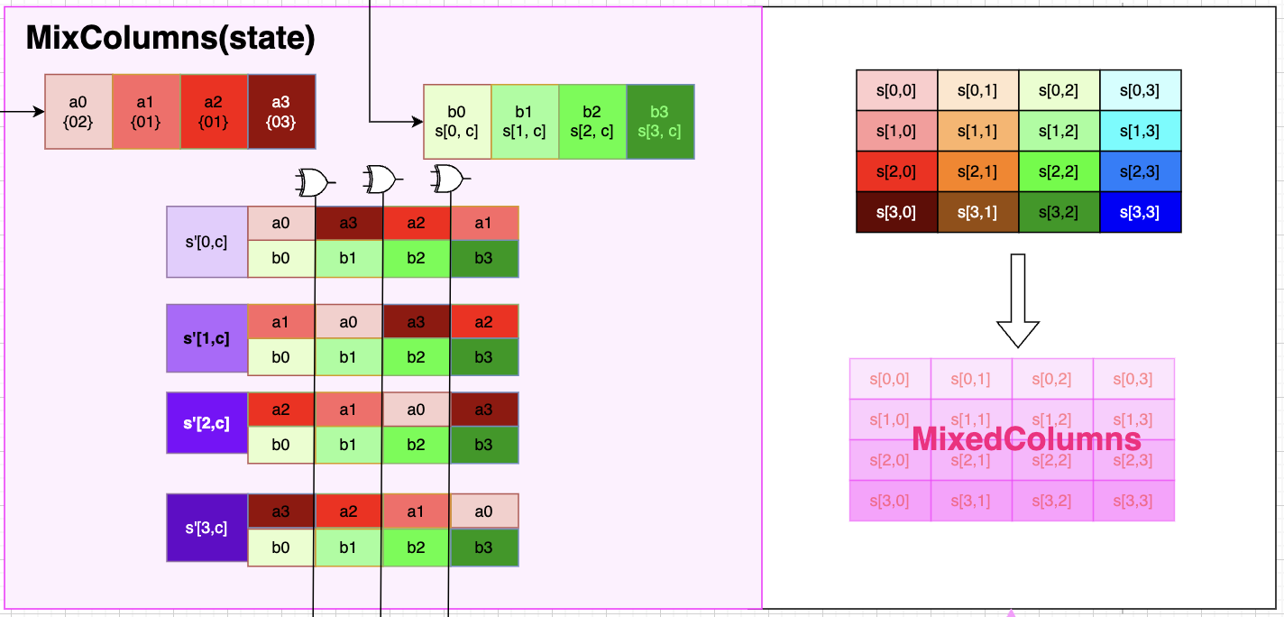
state_primevariable.MixColumns(state) – Recombines a set of columns using a predefined matrix of hexadecimal values.
SubBytes – Uses a function called “sbox” to substitute every word within a matrix with another word. This matrix is unique and causes a high degree of randomness within the completed function.
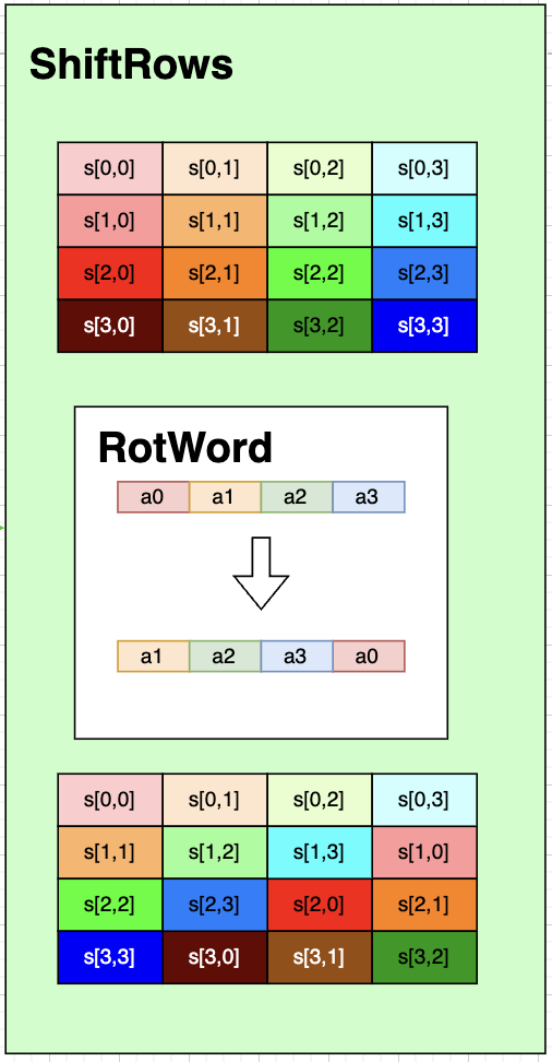
ShiftRows – Considering state as a matrix, shifts all the state values over by one two the left (including wrap around) depending on which row the state is.
KeyExpansion – Defines a new list of words based on a supplied key. For each “round” of the function, new words are created, which are used in other functions to adjust the state.
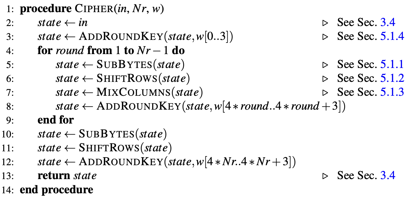
Overall, these functions all come together as described in the pseudocode found on page 12 of the FIPS manual, and can be seen in the image below Figure 1.
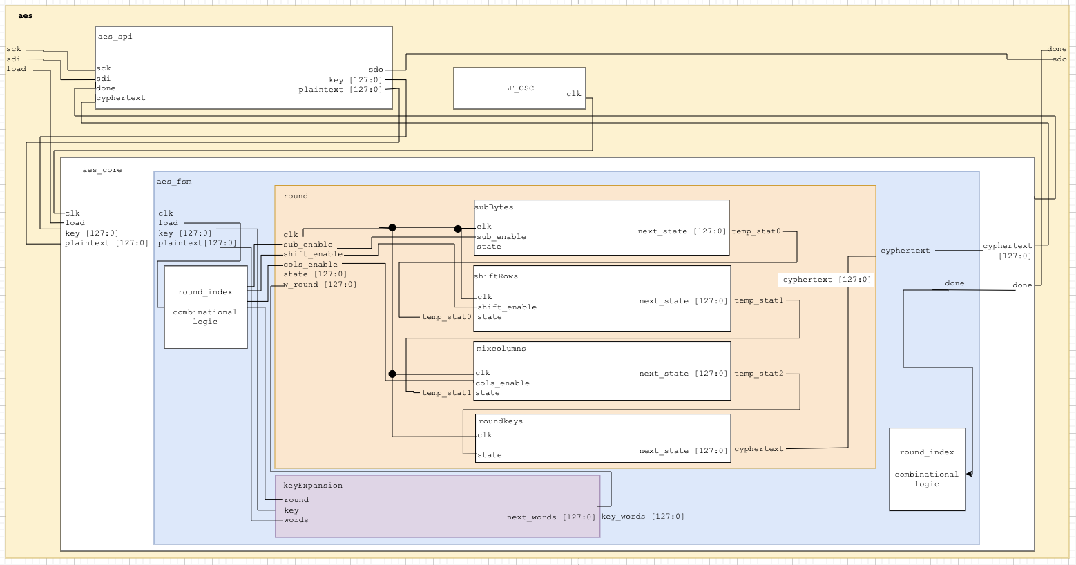
I drew out each progran, and will go into further detail with each of the following diagram for my Radiant Software program.
AddRoundKey(state, w_round)
AddRoundKey is a function that is used to generate the list of words that will be used by the program to alter the incoming key; for each “round” that this cypher goes through, the program will generate a list of words that are dependent upon the initial key supplied to the program.
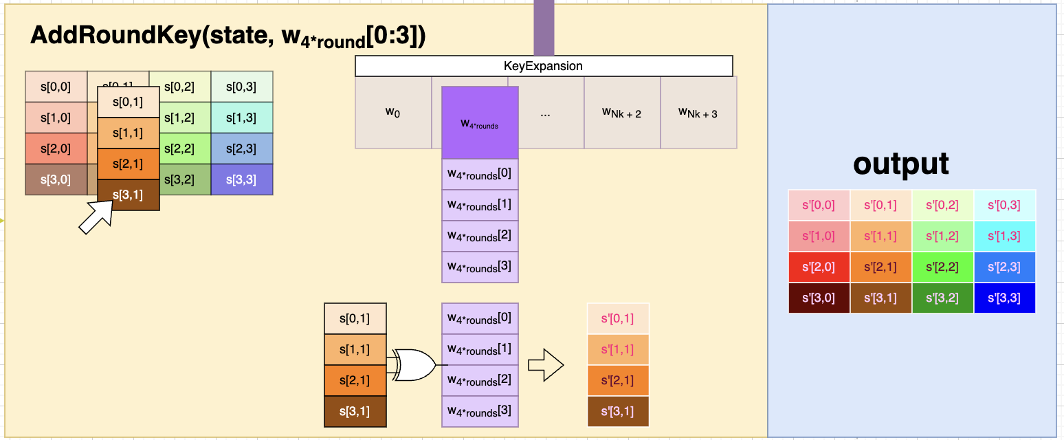
These values are determined with the aid of KeyExpansion Section 1.2.3.
MixColumns(state)
MixColumns is a fucntion that uses a XOR gate to combine a mix of rows combined with a pre-assorted list of values specific to the AES fucntion, in this case AES-128. This mixing is one of the special pieces of AES, as it is hard to decipher without the initial list of values (defined in Figure 2)

For a better perspective on what is happening, I have additionally put together a diagram below that shows the user how this is implemented.
 .
.
KeyExpansion()
KeyExpansion uses XOR and a list of ten pre-defined hexadecimal values to change the incoming list of words and alter them for the use of “AddRoundKey”.
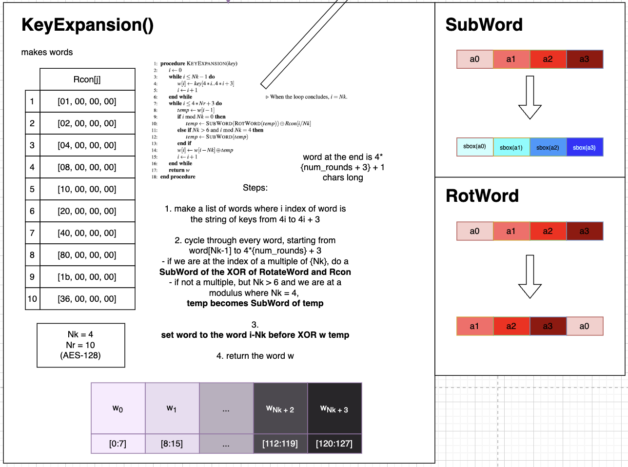
Depending on the round in which the user finds themselves, KeyExpansion will determine the next word using a mix of rotating the words, substituting the words using the SubWord function ( Section 1.2.3.1 ), and XORing values in a specific order.
SubWord
SubBytes is part of the magic of the AES Encryption algorithm, and allows the same value that goes into the matrix, when altered, to be entered again and return its original value. It alters it using something termed “sbox”, where each value is multiplied or combined with some defined list of values. This matrix is extremely large, and as found in the lab, should be implemented using the system’s RAM.
RotWord
The RotWord function is implemented within a multitude of functions to rotate a row of the incoming word (termed as “state” within the pseudocode)
ShiftRows(state)
ShiftRows rotates the incoming word by a differing amount for each row, and as such completely rotates the entire matrix within the function.
SubBytes()
SubBytes uses the synchronized version of SubWord ( Section 1.2.3.1 ) to perform the sbox transformation 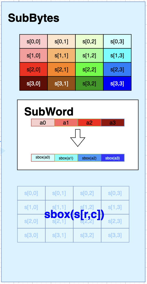
Final Setup
The final design can be represented in the following block diagram. As can be seen in the block diagram, sbox has two potential functions; sbox and sbox_sync. In this case, we need to have a synchronized sbox_sync because there is not enough memory on the FPGA to store the sbox memory before transmitting it. As a result, we need a way to synchronize the sbox in order to prevent its memory from being stored at the same time as other functions so that enough memory is given to the network. This problem with memory mapping can be seen in the image below, where an error message is called due to a Synthesis Error.
As can be seen in the diagram below, despite using synchronized sbox values, all of the RAM on the FPGA is still used by the program and overflows such that most of the registers on the board are used.
Test Bench Trials
The test bench trials did function properly for both the SPI and the CORE; in order to test both of these, however, a series of smaller test benches needed to be crafted to test each function. These were made using the defined table of AES functions as defined in the PDF.
For each function, a set of vectors for the state input and state output were made, and the program was run to confirm that the right value was received. Since there are no such thing as edge cases in many of these functions, I didn’t construct any fringe case scenarios for this problem.
Testing FSM Testbenches can be seen below, with various zooms on the FSM.
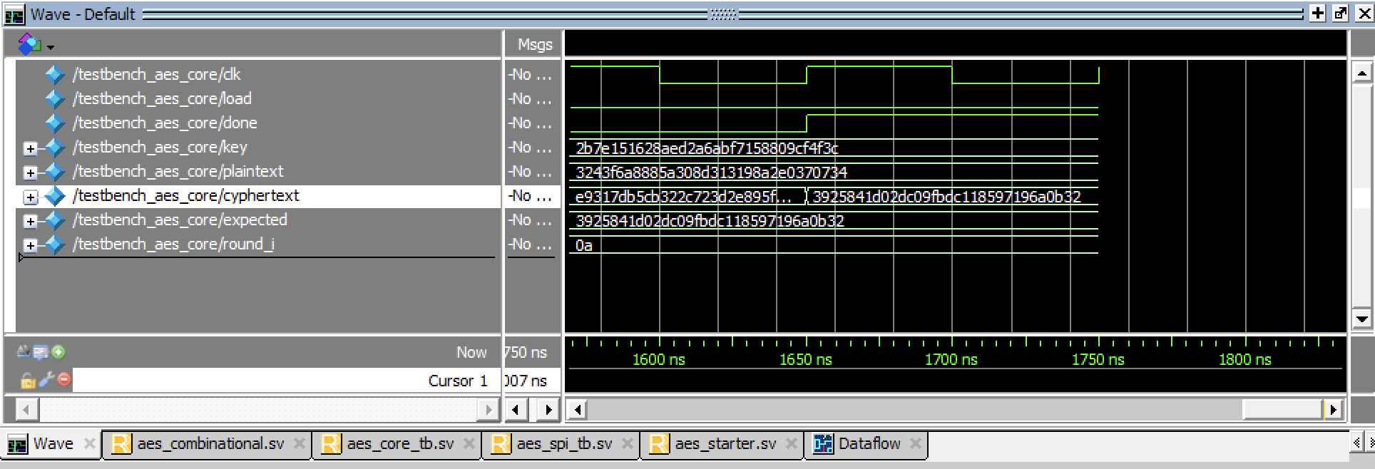
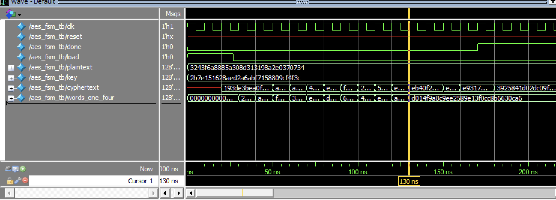
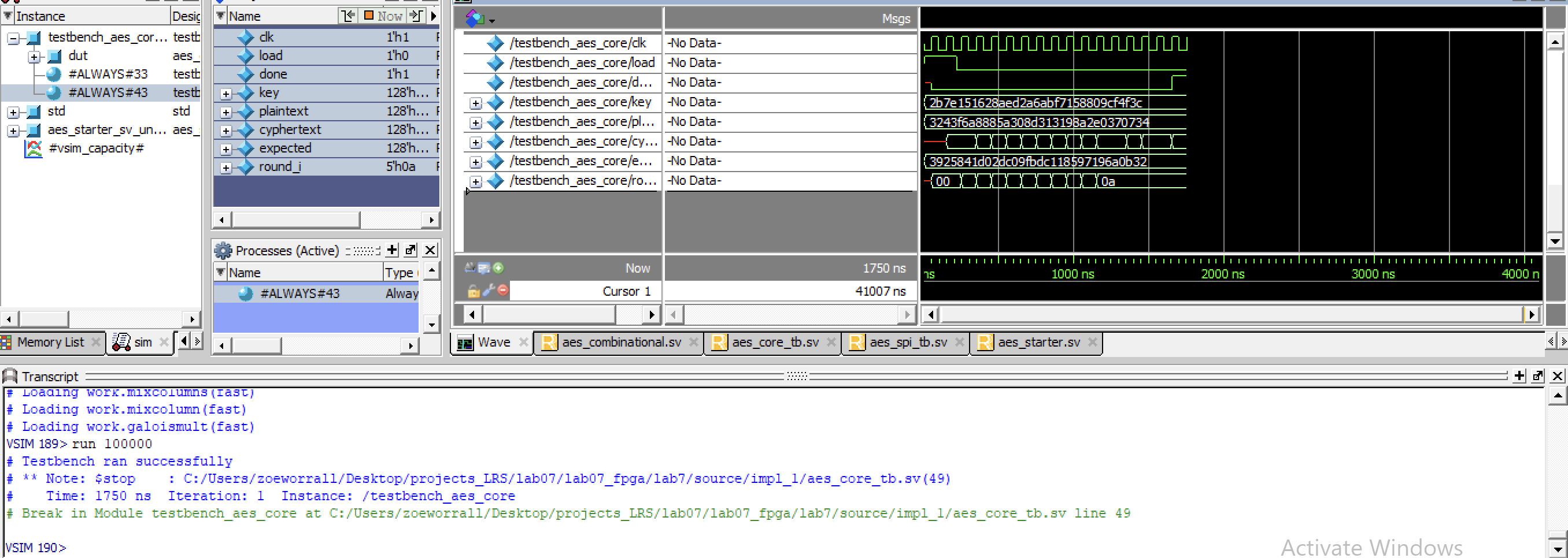


These FSM’s can be further demonstrated to be working by viewing these in the SPI Tesbenches.
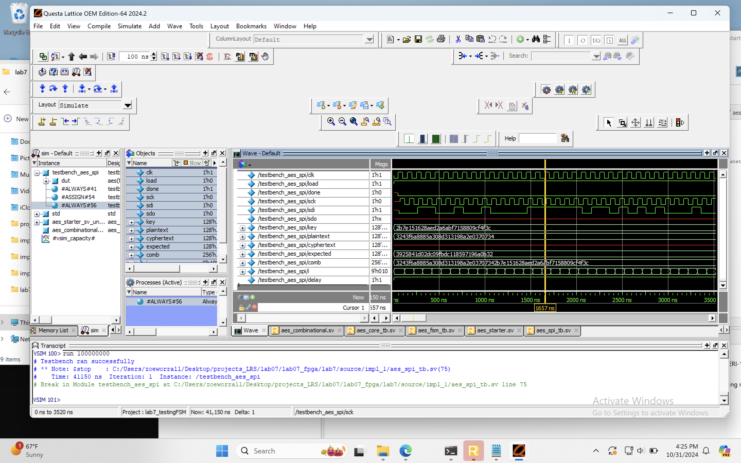
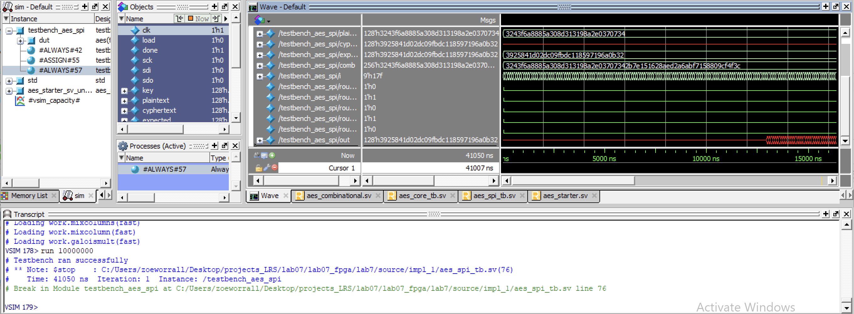
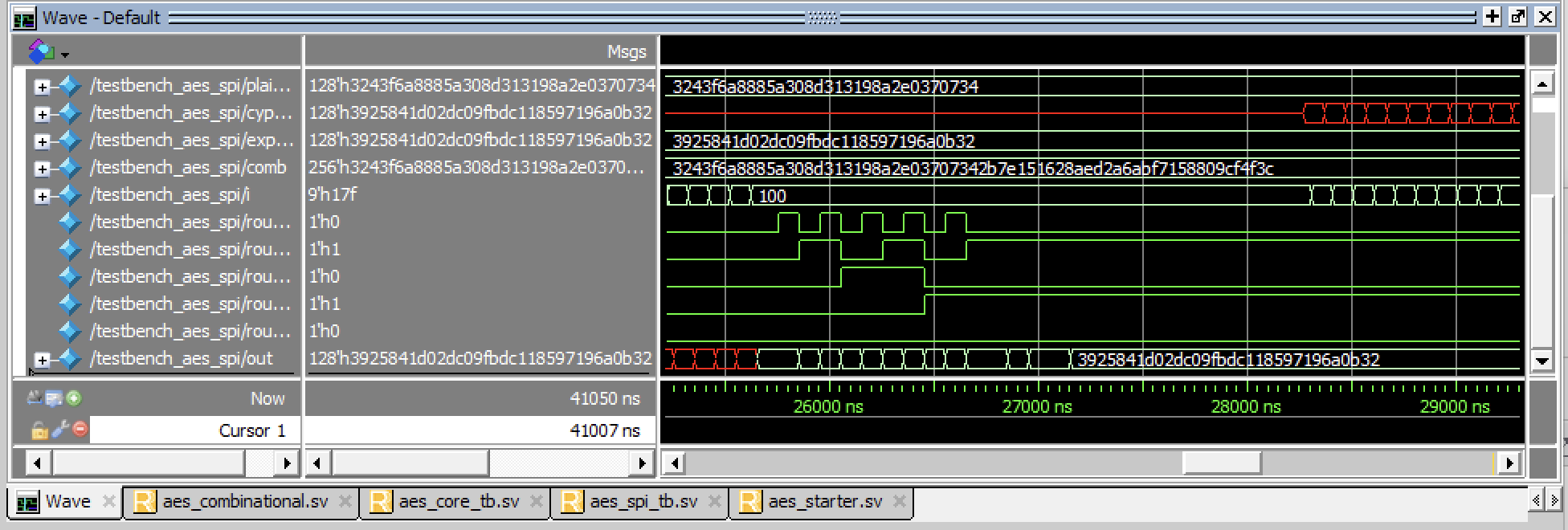
Once all the trials were confirmed to have been working within the testbench, I then moved on to implementing the design onto my actual machine.
Hardware Trials
The following schematic shows how the pin connects on the MCU and FPGA builds look.
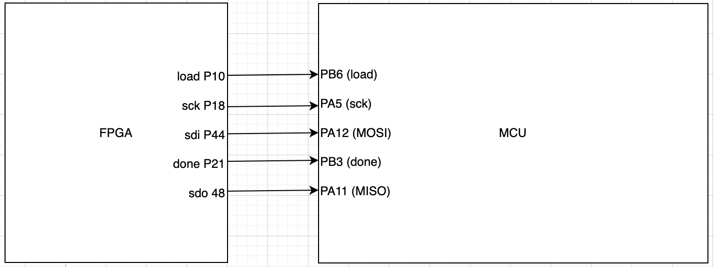
I faced considerable problems with the hardware set up for this lab; I believe that this was, in part, due to a problem with my PB4 and PB5, which are shorted together due to soldering issues. With my Lab 6, I was able to avoid this issue using PB12 and PA11, but due to some of the requisites of this lab, and the time constraints on my own part, I was unable to complete this aspect of the project.
The majority of the time that was stocked up during this project was the time it took to troubleshoot my software to hardware connection. Compiled, three days worth of hours were spent trying to get the hardware working. Multiple variations of code were tried while troubleshooting:
Initially, there was no “DONE” block in my FSM, and as a result my final program may have started in the wrong state. I fixed this by rewriting my FSM and making sure I included a state for each potential block.
I was not initially using the right board, and instead had implemented my program with too few memory blocks; as a result, there were only 12 RAM buckets, and none of the sbox values could fit in them. When I upgraded, this issue was solved.
I initially had 32 rather than 16 sbox modules initialized; this was because I had initialized an SubBytes register both in my fsm machine, to perform an operation before I entered rounds 1-9, and within my “rounds” function. I solved this by including a system of enables in all my functions, which allowed me to toggle what I was receiving out of “rounds”, and resultantly use rounds for every single computation.
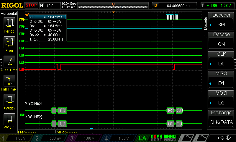
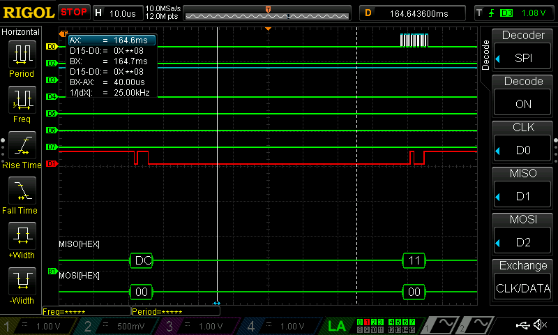
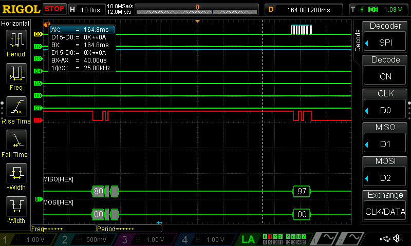
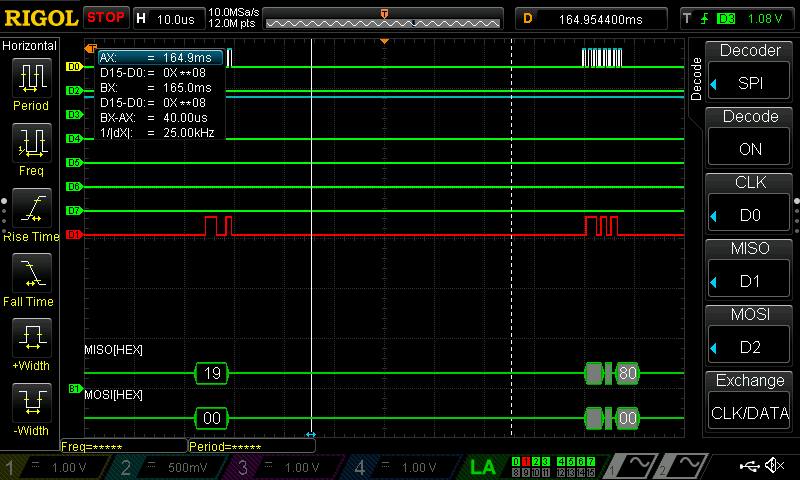
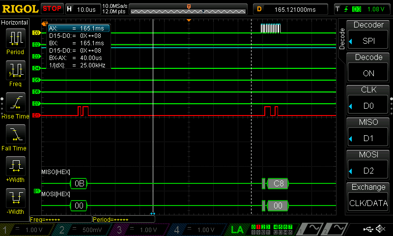
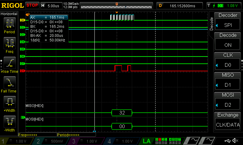
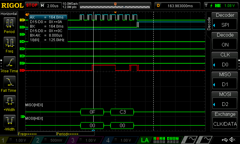
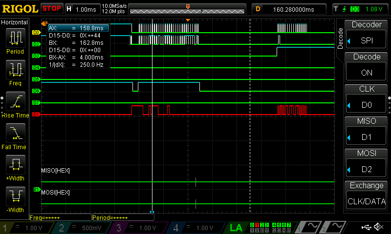
In the end, however, the issue was not my code; I continued running into the same problem, where the SPI was outputting a variety of values, always the same, but varying with time (there were a total of three distinct SPI values that the FPGA was receiving from the MCU). However, when I programmed my code onto another person’s FPGA, my code worked. I confirmed this on two FPGA boards, and confirmed that the software was correct, but something on my hardware was gone.
Results and Discussion
I learned a lot of resilience with this project; there were many points where I wanted to give up, but I would continue trying and experimenting. Even though the trial and error felt wasteful, especially close to the end, I believe I understand AES-128 far better than I ever would have if I had gotten it working on my first run through.
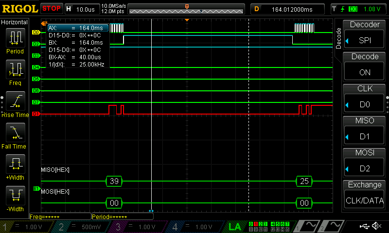
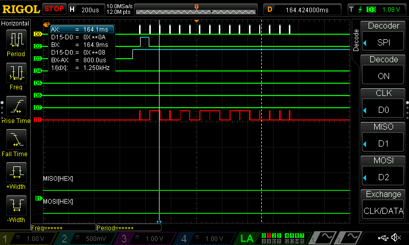
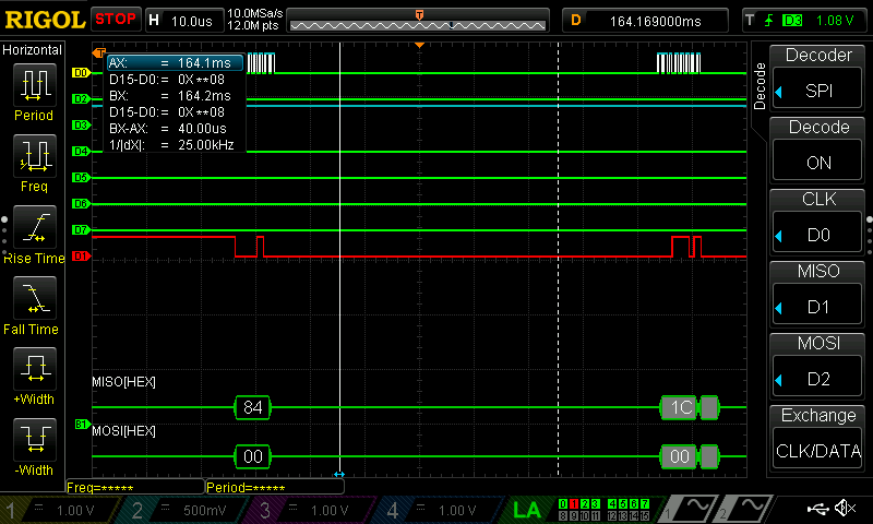
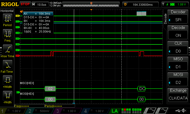
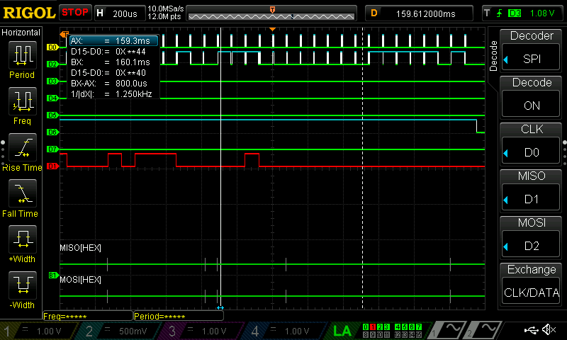
As can be seen below, all of the data was able to be seen with the use of a logic analyzer; I have put these in the listings at the bottom of this page.
Additionally, in the future I would like to examine my FPGA with a Logic Analyzer to troubleshoot what’s wrong with the pins, and what may be shorted together on my board.
Conclusion
In conclusion, after many long hours, I can consider this Lab a success. I think that AES encryption and SPI communications will always be difficult to understand, but with this Lab I’ve gotten proof that I can succeed by working hard.
