Lab 4 Writeup
Lab 4: Digital Audio
Hours Spent: 48.6, Mapped with Toggl Track
Introduction
In this lab, a STM32L432KCU Microcontroller Unit (the MCU) was used to control a SM231508-1 Speaker to play a series of different musical songs. In order to do so, the MCU was programmed to control the E155 Breadboard Adapter v4 board to output voltages on GPIO pins using an internall phase-lock looped clock, as well as two timers. Through the design of several structs, the enabling of cross communication between pins, and careful reading of the datasheet, the microcontroller was configured to play songs like “Fur Elise” as well as “Megalovania” and several other recognizable game tunes.
Design: Modules
Code Layout
Segger Embedded Studio 8.16a was used to program all modules. In order to do so, it was necessary to first find all relevant and necessary components for this lab, as well as compile a series of libraries that would be used in its construction. Of note, we were explicitly told to not use the inbuilt stm32l432xx.h header file from the Segger’s library; we wrote all headers and c code for this class from scratch to ensure that we understood all necessary components.
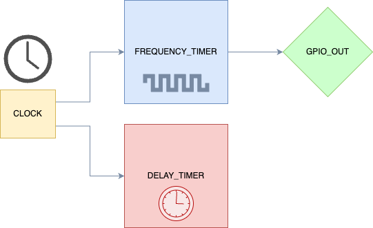
The system that was designed for this lab required this simple framework (Figure 1) to function: the main point was that a clock (CLOCK) would be generated and sent into two timers (FREQUENCY_TIMER and DELAY_TIMER); the first would control the frequency of the speaker (GPIO_OUT), the second would control for how long the frequency was played. As a result, we would need to make four c files:
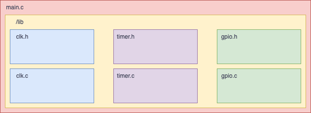
main.c: a C file that sits above all the headers and other c files in order to properly assign the enable pins and run the actual music itself.
clk.c/clk.h: A paired C and C header file that assign the proper variables and memory allocations for running clocks onboard the MCU. This looks specifically at pages 175-246 of the STM Reference Manual to assign all relevant materials. Further details of what needed to be assigned of this can be found in Clock Memory and Layout (Section 1.2.1.1).
timer.c/timer.h: A paired C and C header file that assign the proper variables and memory allocation for running timers onboard the MCU. It uses logic gathered from pages 817-980 in the STM Reference Manual and pages 51-58 in the STM32L432xx Datasheet. Further details of what needed to be assigned of this can be found in Timer Layout.
gpio.c/gpio.h: A paired C and C header file that assign the proper variables and memory allocation for connecting to GPIO pins onboard the mcu. It uses logic gathered from pages 258-275 in the STM Reference Manual. Further details of what needed to be assigned of this can be found in Timer Layout (Section 1.2.1.3).
This expanded out into the final, overarching layout seen in Figure 2.
Clock Memory and Layout
Before programming anything, all necessary parameters to control a clock were written out using Figure 13 in the Reference Manual. For this specific scenario, I wanted to control the phase-locked loop clock to gain experience with varying an onboard clock within the program. This required the layout of the memory bank (based on pages 243-246 in the Reference Manual), as well as the variables assigned as indicated in Table 1 and Table 2. In order to easily access each memory bit, I set up a structure within the header file (called RCC_STM32L432xx_TypeDef), which I then built off the RCC base located at 0x40021000UL to control each individual register on the MCU. There are two functions for this program: configurePLL and configureClock; configurePLL sets up the PLL to be connected to the onboard MSI clock, and configureClock sets up a clock to be delivered to the rest of the board.
| Variable Name | Variable Assignment | Variable Location | Purpose |
|---|---|---|---|
| PLLON (beginning of configurePLL) | 0 at bit 24 | RCC, Configuration Register (CR) | So that the clock can be properly reconfigured, it must be turned off |
| PLLRDY | not assigned, but wait until its 0 | RCC, Configuration Register (CR) | Wait to make sure you can reprogram this bit |
| PLL_SRC | 1 at bit 0 | RCC, PLL Configuration Register (PLL_CFGR) | Turning on PLL and connecting it to the MSI (40 MHz) internal clock |
| PLLR | 0b00 from bits 25:26 | RCC, PLL Configuration Register (PLL_CFGR) | Dividing the incoming clock (MSI) by a factor of 2 |
| PLLM | 0b000 from bits 4:6 | RCC, PLL Configuration Register (PLL_CFGR) | Dividing the output clock (Voltage Controlled Oscillator Output) by 1 |
| PLLN | 10 from bits 14:18 | RCC, PLL Configuration Register (PLL_CFGR) | Multiplying the output clock by 16 |
| PLLON (end of configurePLL) | 1 at bit 24 | RCC, Configuration Register (CR) | So that the PLL is now running again, reconfigured |
| PLLCLK | 1 at bit 24 | RCC, PLL Configuration Register (PLL_CFGR) | So that the PLL is sent out of the register as the internal clock |
| Variable Name | Variable Assignment | Variable Location | Purpose |
|---|---|---|---|
| SW | 0b11 at bits 0:1 | RCC, Configuration Register | To set up the output clock to be PLL |
| SWS | 0b11 at bits 2:3 | RCC, Configuration Register | To make sure that the PLL has been configured on, we wait for this to be 1 |
Timer Layout
For this specific scenario, I wanted to control two timers (as specified in Figure 1), one that would be used to control the frequency of the speaker, and the other that would be used to control how long the frequency was played. This required the layout of the memory bank (based on pages 814-816 in the Reference Manual), as well as the variables assigned as indicated in the Expandable Table. In order to easily access each memory bit, I set up three structures within the header file for Timers 2 and 3, Timers 15 and 16, and Timers 6 and 7 (since each has some variables unassigned, and I didn’t want to accidentaly assign the wrong bits if I happened to be writing to the wrong clock on accident). These structures are called TIM_67_STM32L432xx_TypeDef (Timers 6 and 7), TIM_ALL_STM32L432xx_TypeDef (Could apply to any timer, but is constrained in potential variables for more complex operations (i.e. runs all timers similar to timers 6 and 7)), TIM15_STM32L432xx_TypeDef (Timer 15), and TIM_23_STM32L432xx_TypeDef (Timers 2 and 3). Of these, I built all Timers as defined by their memory as found in Table 2, page 68 and 69 of the reference manual (placed below).
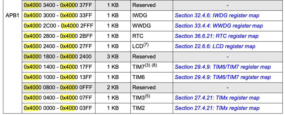
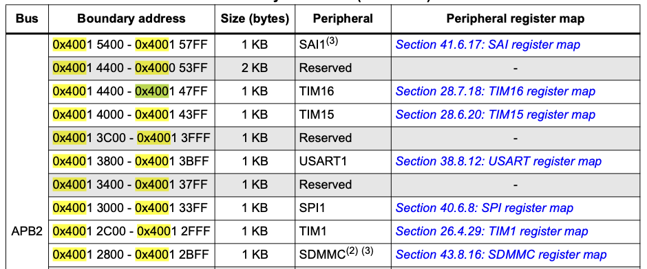
The variables were assigned for the following values in order to run: in total, I have four functions: delay(TIM_67_STM32L432xx_TypeDef * DELAY_TIMx, uint32_t time), configure_TIM23_PWM(TIM_23_STM32L432xx_TypeDef * TIMx, int freq, double duty), configure_TIM2_CH1_PWM(int freq, double duty), and configure_TIMx(TIM_67_STM32L432xx_TypeDef * TIMx). Each of these functions is meant to set up a timer or perform a function using said timer. configure_TIM23_PWM is meant to set up either Timers 2 or 3 acting in PWM mode. configure_TIM2_CH1_PWM was created to control specifically timer TIM2, and noticeably does not take in an input TypeDef clock. There is an additional function within the C file with a similar name, which overloads this function, and performs a similar function but with a predecided frequency and duty cycle for the timer, which was used to organize when designing the other functions; it cannot be called from the main C function. configure_TIMx is meant to set up a given timer to begin running in counter only (since it is for Timers 6 and 7, which cannot generate their own outputs). Finally, delay assumes that the user is using configure_TIMx to design a timer, and with the predetermined parameters for this function (i.e. generates a signal at 77 kHz), waits for time number of miliseconds. I will specify only the variables as defined in the configure_TIM23_PWM function, as this is what is used within the program to setup the desired frequencies for the speaker’s singing, and all the logic used for the configuration of CNTR, ARR, and CCR is used for setting up TIM6.
| Variable Name | Variable Assignment | Variable Location | Purpose |
|---|---|---|---|
| CC1S | 0b00 at bits 0:1 | Capture/Compare Register 1 (CCR1) | Configure Channel 1 of the clock as Output |
| OC1M | 0 at bit 16, 0b111 at bits 4:6 | Capture/Compare Register 1 (CCR1) | Configure the timer in PWM mode 2 (i.e. high when the counter is greater than the assigned CCR value) |
| CC1E | 1 at bit 0 | Capture/Compare Enable Register (CCER) | Set OC1 as the active channel |
| CC1P | 0 at bit 1 | Capture/Compare Enable Register (CCER) | Make OC1’s “active” be 1 (i.e. when its “on”, its output voltage) |
| ECE | 0 at bit 14 | Slave Mode Control Register (SMCR) | Sets the external clock to 0 to make sure that we are using the internal clock for this timer |
| SMS | 0 at bit 16, 0b000 at bits 0:2 | Slave Mode Control Register (SMCR) | Sets the internal clock to be used when CEN is enabled |
| ETF | 0b011 at bit 8 | Slave Mode Control Register (SMCR) | Sets the external trigger factor such that it divides the input clock by 8 |
| PSC | 256 | Prescaler Register | Sets the input clock to be divided by 256 (slowing the timer down) |
| ARR | 9 kHz / desired frequency | Auto-reload Register (ARR) | Sets the value the counter will get to (sets frequency of timer) |
| CCR1 | duty cycle * ARR’s value | Capture/Compare Register 1 (CCR1) | Sets the value the counter is compared against (generates output and duty cycle) |
| OC1PE | 1 at bit 3 | Capture/Compare Mode Register 1 (CCMR1) | Enables the preload for this channel. Necessary for PWM mode unless configure in One-Pulse mode |
| ARPE | 1 at bit 7 | Control Register 1 (CR1) | Enable the auto-reload preload feature |
| CC1G | 1 at bit 1 | Event Generation Register (EGR) | Enable the Capture/Compare 1 Generator |
| UG | 1 at bit 0 | Event Generation Register (EGR) | Enable the update generation; this will allow us to continue counting over and over via taking advantage of the shadow preload registers |
| CMS | 0b00 at bits 5:6 | Control Register 1 (CR1) | Set the timer to work in edge-aligned mode |
| DIR | 0 at bit 4 | Control Register 1 (CR1) | Set the counter to be an upcounter |
| CEN | 1 at bit 0 | Control Register 1 (CR1) | Enable the counter |
:Timer Commands Table{tbl-colwidths=“[10,30, 30,50]”}
GPIO Layout
There are two primary things that need to be done to set up the GPIO pins on board the MCU: the first is that they are set up in a mode that can communicate with the timer (in this case, I chose to use Alternate Function 1, which allows PA5 to communicate with Timer 2’s Channel 1), and the second that the pin is enabled. There are four functions within my gpio.c class, but in this instance only one of these functions is necessary, the setModeOfPinA function. This function sets the GPIO’s mode into the “alternate function” mode, which will allow certain pins to interact with other on-board pins.
To do this, the MODER register of the GPIO structure that I constructed in header needs to have the two bits that refer to the GPIO pin on the board set to 0b10: after this, AF logic assigned within the main function will be able to correctly interact with and assign values to the pin.
Main Function
The final C file of this lab is the main.c, which compiles all of the code together. Inside, it calls the configureClock function (which calls configurePLL), sets the mode of the pin, configures the timers, and connects the clocks to the timers and the pins. Finally, it also assigns the alternate function desired to the pin via the low alternate function register (GPIOA - AFRL); I referred again to Table 15 in the MCU Datasheet.
Math for Frequency Calculations
The frequencies generated by the speaker were confirmed to be accurate through the use of an iPhone tuner app “Tuner T1”, and via calculations for each of the relevant frequencies and time delays.
Timer 2 was used to generate frequencies. Because it has both a prescaler and the internal variable ETF (external trigger factor), it was able to divide the incoming frequency (in this case, the 20MHz generated by the PLL timer) twice. The PSC was set to be 32, and the ETF to be 8, which effectively scales the timer to run at a 75757.58 Hz. The frequencies that it is able to send the speaker, then, vary depending on the size of the array, and potentially additional configurations you can make to the duty cycle. The highest frequency that could be produced using this PSC and ETF setup \[ \frac{75757.58}{2} Hz = 37878.79 Hz \]
This is because the speaker must be turned off and on to generate one full wave; in order for a full period to pass, the output must be turned off and on again, meaning that CCR1 would be set to 1, and ARR would be set to 2 in this scenario.
The lowest frequency possible with this clock would be one where the counter counts to the maximum value of ARR. I am currently assuming that the user may chose to use Timer 2 or Timer 3, so although Timer 2 could have an array of up to \(2^{32} - 1\) counts, I will first consider both Timers together (where Timer 3 is constrained to 16 bits). In this scenario, the maximum that the counter could ever reach would be \(2^{16}-1\), or 65535. In this case, the lowest possible frequency would be given by
\[ \frac{75757.58}{65535} Hz = 1.16 Hz \]
However, I would also like to consider possible future reiterations of this design that could allow for even more flexibility with frequency and duration: in the case where we only use Timer 2, and we include the 32 bits that Timer 2 can use for ARR, the lowest possible frequency is 17.64 µHz. If we additionally consider that we could arrange an additional function that sets the output to its inverse whenever the counter is set (effectively creating a 50% duty cycle for half the frequency), we would be able to get either 0.578 Hz for the 15 bit timer, or as low as 8.82 µHz for the 32 bit timer.
As it appies to the accuracy of the timer, the timer should be within 1% of of a given frequency relative to 1000 Hz; because it is an integer value, sometimes values may be clipped for the frequency. However, this is a minimal amount of frequency clipping. 1% of the frequency range, in this case is given by
\[ \frac{1000-220}{100} = 7.8 Hz \]
In order for the frequency to be within 1% of 220 Hz, for example, it would need to be between about 213 and 227 Hz. With our current frequency, the integer division of our clock frequency over time would mean that each square wave would happen over a period of \(\frac{75757.58}{220} = 344.4\) counts. If this is rounded to the nearest integer using the ceil function in C (i.e. 344), the actual Hz that would be generated by the speaker would be 220.2 Hz, well within our required frequency limit. If we go to the maximum Hz range, we can see that the final length of the cycle would be \(\frac{75757.58}{1000}\) or 75.75 counts, which would become 76. In this case, the final generated frequency would be 996.81, which is 0.4% from it’s intended value relative to the range (using \(\frac{1000-996.81}{1000-220} = 0.4%\)), which inside our desired 1% range.
As for the delay timer, I currently have it configured so that it prescales by 512. Because there is no external filter trigger in this instance, we do not divide by any additional values, and so the frequency of the counter within TIM6 is given by \[ \frac{20}{512} MHz = 39 kHz \]
The shortest possible delay for this timer would resultantly be the length of one counter, i.e. 1/39 kHz, which in this case is 25.6 µs. In the case that we would like it to last as long as possible, the longest period would be when \(2^{16} - 1\) clock cycles occur (i.e. ARR = 65535), which would mean a longest period of 1.678 seconds. In our case, since we are playing music that has, at maximum, a whole note that lasts a second, all the music is well within the range of possible note lengths.
Hardware Setup
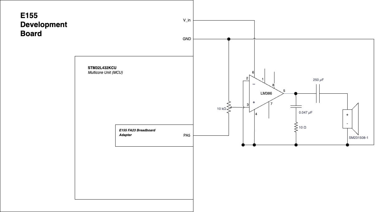
The hardware setup for this lab was relatively simple. Because the speaker requires a greater current that the MCU GPIO pins can provide, I used an LM386 amplifier to set-up my system. This chip was set up for a gain of 50 (relative to Figure 9-5 on the data sheet), and has a 10k potentiometer place at the output of pin 3 in order to control the volume of the speaker Figure 3.
Initial Testing
Because this lab required the implementation of multiple parts, I used two strategies to confirm that my code was working as expected. The first was the “Build and Debug” mode that is found inside of Segger Embedded Studio, which allows you to see the internal memory of the MCU as its running. With this, I was able to confirm when my counter was working, and additionally catch bugs. Some relevant bugs that I caught using this strategy were:
I did not initially realize that Timer 2 had 32 bits, and resultantly the CCR1 was consistently being set to a negative value. This meant that counter was always greater than CCR1, and because it was set to output high when this was the case (PWM mode 2), the LED never turned off. After setting the values within counter (CNTR), ARR, and CCR1 to display their decimal values, I realized that CCR1 was displaying a negative number, and so I altered the upper bits of both ARR and CCR1 so that they were not negative.
For a long time I was not able to get the output traveling to GPIO A. I noticed while debugging that GPIO was not updating at all, even though I had confirmed before adding the timer that it was able to update. When I cross-checked my code with a demo I made to blink the LED, I quickly realized that I had accidentally set the GPIO B pins, not the GPIO A ones.
For an additional form of testing, specifically to confirm that I was seeing the anticipated frequencies, I hooked up an LED to my output in order to observe it blinking at low Hz. This helped me confirm that the calculations that I had made for the frequencies were correct (i.e. the delay of 1 second worked, and that the frequency of blinking was similarly accurate). Although there are no test benches for this program, I believe that in the end this worked effectively to debug my system as a whole.
Results and Discussion
In conclusion, this lab was a success in configuring an MCU board using C headers and functions. It additionally provided insight into the internal structures and memories found on an MCU, as well as provided a comprehensive understanding of all the relevant background required for working with MCU (Figure 4).
Video of Working Speaker
Conclusion
In conclusion, all of the program works properly in simulation and in hardware, and can be confirmed both visually and with the aid of a test bench. The program is able to multiplex successfully without having the two LEDs bleed over, and all digits are equally lit for each segment, and proper calculations for the PNP transistor can be found above.
I spent a total of 48.6 hours working on this lab, with roughly seven of them spent on the lab writeup, and three spent on fixing the github repo that I broke by uploading a video that was too big, if including the planning of the modules and compiling all of the necessary diagrams.